CARY, NC--(Marketwired - May 28, 2013) - Coventor®, Inc., the leading supplier of virtual fabrication solutions for semiconductor devices and micro-electromechanical systems (MEMS), today announced immediate availability of the SEMulator3D® 2013 software platform. SEMulator3D 2013 brings unprecedented physical accuracy and predictive modeling capabilities to process development and integration. This milestone release expands the value of 'virtual fabrication' to the broader semiconductor ecosystem in order to dramatically reduce silicon learning cycles and the billions of dollars spent reaching manufacturing readiness.
SEMulator3D 2013 release comes at a particularly critical time for semiconductor companies grappling with the complexities of integrated 3D front-end-of-line (FEOL) manufacturing processes such as Tri-Gate and High-k/Metal Gate logic, as well as advanced 3D memory technologies. Fabless design teams also face tremendous challenges migrating their intellectual property (IP) into these new technologies. SEMulator3D 2013 responds to such evolving requirements with an advanced virtual fabrication platform that makes it possible for foundry and fabless development teams to effectively collaborate at the physical process level.
"With new silicon architectures ramping quickly, IBM is introducing new manufacturing technologies that will keep us on the cutting edge of chip-making for server microprocessors, systems-on-chips and specialty silicon for consumer applications," said Gary Patton, Vice President, IBM Semiconductor Research & Development Center. "Tools such as Coventor's SEMulator3D Virtual Fabrication platform have allowed us to speed our end-to-end technology development in 22nm and beyond, enabling a faster time to market for our customers who depend on IBM innovation to create the latest servers, smart phones, GPS systems, routers and other devices."
At the core of the new SEMulator3D 2013 platform is a revolutionary physics-driven modeling paradigm for addressing physical process behavior that makes virtual fabrication more predictive and provides new opportunities for replacing actual silicon learning cycles with faster, less costly virtual cycles. In addition, virtual metrology innovations and the automation of virtual experiments enable process developers to perform virtual fabrication operations in hours or days instead of the months required for actual silicon learning cycles.
"Time and complexity challenges are the two constants in semiconductor design and manufacturing, and the growing trend toward 3D integrated technologies like FinFETS has introduced unprecedented levels of pain in both areas. SEMulator3D 2013 addresses the need for more efficient, automated approaches to process modeling, as well as the need for greater levels of collaboration by both ends of the development process. The net result is a dramatic reduction in the time and cost required to leverage the most advanced manufacturing techniques required to keep pace with Moore's Law and fuel even more innovation across the electronics industry," according to Dr. David Fried, Chief Technology Officer at Coventor.
The impact of SEMulator3D 2013 breakthroughs will be showcased with live software demonstrations in Coventor Booth #1326 at the 50th Design Automation Conference, June 2 to June 6, 2013 in Austin, TX and a technical presentation by Coventor CTO Dr. David Fried on "Virtual Fabrication: Integrated Process Modeling for Advanced Technology" at SEMICON West that takes place in San Francisco, CA from July 9 to July 12, 2013.
Setting New Standards for Physical Accuracy
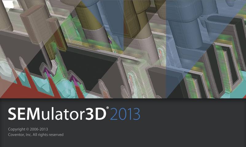
SEMulator3D 2013 features a new surface evolution engine and seamlessly combines the benefits of advanced physics-driven and high-speed behavioral ('voxel') predictive modeling in a single, easy-to-use platform. Voxel modeling is a fast, robust digital approach capable of scaling to the requirements of integrated processes and large silicon areas. Surface evolution is a more analog approach capable of modeling a wide range of physical process behavior.
Coventor's unique deployment of surface evolution facilitates a major step forward in modeling reactive ion etching and selective epitaxial growth, a key technique for creating channel stress in advanced planar and FinFET technologies. With SEMulator3D 2013, users can model etching of multi-material stacks with multiple types of etch physics, such as redeposition (passivation), sputtering (physical etching), and etch bias (lateral or chemical etching). They can also model the growth rates of major silicon plane families to predict the faceted shapes and structural ramifications of selective epitaxial growth.
Advanced Automation Technologies
The SEMulator3D 2013 platform incorporates advanced technologies and tool enhancements that enable automatic process variation analysis with parallel modeling and virtual metrology to significantly increase user productivity. A new spreadsheet-driven Expeditor tool for batch processing enables massively parallel parameter studies. The addition of new virtual metrology steps into the virtual fabrication process provide for in-line, local measurement of critical dimensions, mimicking actual metrology operations. Tool upgrades include an enhanced Materials Editor for hierarchical grouping of materials, which greatly simplifies process deck development and maintenance.
Availability
The SEMulator3D 2013 release is shipping today.
About Coventor
Coventor, Inc. is the market leader in automated design solutions for micro-electromechanical systems (MEMS) and virtual fabrication of MEMS and semiconductor devices. Coventor serves a worldwide customer base of integrated device manufacturers, fabless design houses, independent foundries, and R&D organizations that develop MEMS-based products for automotive, aerospace, industrial, defense, and consumer electronics applications, including smartphones, tablets, and gaming systems. Coventor's software tools and expertise enable its customers to simulate and optimize MEMS device designs and fabrication processes before committing to time-consuming and costly build-and-test cycles. The company is headquartered in Cary, North Carolina and has offices in California's Silicon Valley, Cambridge, Massachusetts, and Paris, France. More information is available at http://www.coventor.com.
Coventor and SEMulator3D are registered trademarks of Coventor, Inc. All other trademarks are the property of their respective owners.
Note to Editors: Digital images are available.
Contact Information:
For more information, contact:
Mike Sottak
(408) 876-4418